K2608 Datasheet PDF – 900V, 3A, N-Ch, MOSFET, 2SK2608

Part Number: K2608, 2SK2608

Function : 900V, 3A, Silicon N Channel MOSFET

Package: TO-220AB Type

Manufacturer: Toshiba

Image

K2608 mosfet

Description

This is 900V, 3A, Silicon N Channel MOS Type Field Effect Transistor.


Features

1. Low drain−source ON resistance  : RDS (ON)= 3.73 Ω(typ.)

2. High forward transfer admittance  : |Yfs|=2.6 S (typ.)

3. Low leakage current  : IDSS= 100 μA (max) (VDS= 720 V)

4. Enhancement mode  : Vth= 2.0~4.0 V (VDS= 10 V, ID= 1 mA)


Pinout

K2608 datasheet pinout

Absolute Maximum Ratings

1. Drain−source voltage : VDSS = 900 V

2. Drain−gate voltage (RGS= 20 kΩ): VDGR = 900 V

3. Gate−source voltage : VGSS = ±30 V

4. Drain power dissipation (Tc = 25°C) : PD = 100 W

5. Single pulse avalanche energy : EAS = 295 mJ

6. Drain current : Id = 3 A

Applications:

1. Switching Regulator

K2608 Datasheet PDF


Related articles across the web

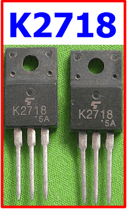
K2718 Datasheet – 900V, N-Ch MOSFET – Toshiba

K2718 is one of the types of MOSFETs and is a kind of transistor.

Part Number: 2SK2718

Function: Silicon N Channel MOSFET

Package: TO-220 Type

Manufacturer: Toshiba

Image

K2718 mosfet

Description

The K2718 is a high-voltage N-channel MOSFET designed for power switching applications, featuring a 900V drain-source rating and 2.5A current capability in a robust package. It offers moderate RDS(ON), high forward transfer admittance, and low leakage current, making it suitable for efficient high-voltage operation. This device is commonly used in DC-DC converters, motor drives, and other high-voltage switching circuits.

Features

  • High drain-source voltage rating up to 900V
  • Low RDS(ON) of approximately 5.6Ω (typ.)
  • High forward transfer admittance |Yfs| of 2.0S (typ.)
  • Low leakage current IDSS up to 100µA at high voltage
  • Enhancement mode operation with Vth between 2.0V and 4.0V
  • Suitable for high-voltage switching applications

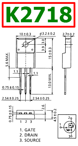
Pinout

K2718 datasheet pinout

Design Notes

  • High RDS(ON) compared to low-voltage MOSFETs requires careful efficiency consideration
  • Gate drive voltage should be sufficiently high to fully enhance the device
  • Suitable for high-voltage applications but switching losses must be evaluated
  • Ensure proper heat sinking for sustained operation near maximum power
  • Avalanche rating allows limited inductive load handling without external protection

Absolute Maximum Ratings (Tc = 25 °C)

Parameter Symbol Value Unit
Drain-Source Voltage VDSS 900 V
Drain-Gate Voltage VDGR 900 V
Gate-Source Voltage VGSS ±30 V
Drain Current ID 2.5 A
Power Dissipation PD 40 W
Single Pulse Avalanche Energy EAS 216 mJ

How to Choose This Part

  • Select for high-voltage applications requiring up to 900V blocking capability
  • Suitable for moderate current switching applications
  • Evaluate conduction losses due to relatively high RDS(ON)
  • Ensure compatibility with available gate drive circuitry
  • Consider switching frequency and thermal constraints

Applications

  • DC-DC converters
  • Motor drive systems
  • Switch-mode power supplies
  • Industrial power control circuits
  • High-voltage switching systems

Alternative / Equivalent Products

  • STP9NK90Z 900V N-channel MOSFET
  • FQP9N90C high-voltage MOSFET
  • IRF840 500V MOSFET for lower voltage applications
  • TK10A90D super junction MOSFET
  • IXTP2N100D high-voltage MOSFET alternative

K2718 Datasheet