The A1015 PNP transistor has a maximum current rating of 150mA, which means it can handle up to 150 milliamps of current flowing through the transistor.
Part Number: A1015
Function: -150mA, -50V, PNP General Purpose Transistor
Package: TO-92 Type
Manufacturer: Toshiba
Image :
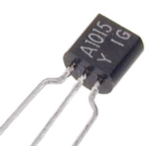
Description
This a PNP transistor, which means it is designed to allow current to flow from the emitter to the collector when a positive voltage is applied to the base. It is commonly used for small-signal amplification and switching applications.
The A1015 transistor has three pins: the emitter, base, and collector. The emitter is the pin closest to the flat side of the transistor, the base is the middle pin, and the collector is the pin farthest from the flat side. The pinout can also be identified by looking at the datasheet of the transistor.
Features
0. Frequency range: The A1015 transistor can operate over a wide frequency range of up to 150MHz. This makes it suitable for use in a variety of applications, including high-frequency amplification, oscillators, and mixers.
1. High voltage and high current : VCEO = -50 V (min), IC = -150 mA (max)
2. Excellent hFElinearity :
(1) hFE (2)= 80 (typ.) at VCE= -6 V, IC= -150 mA
(2) hFE(IC= -0.1 mA)/hFE(IC= -2 mA) = 0.95 (typ.)
3. Low noise: NF = 1dB (typ.) (f = 1 kHz)
4. Complementary to 2SC1815.
Pinout
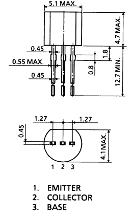
Absolute Maximum Ratings (Ta = 25°C)
1. Collector-base voltage : VCBO = -50 V
2. Collector-emitter voltage : VCEO = -50 V
3. Emitter-base voltage : VEBO = -5 V
4. Collector current : IC = -150 mA
5. Base current : IB = -50 mA
6. Collector power dissipation : PC = 400 mW
7. Function temperature : Tj = 125 °C
8. Storage temperature range : Tstg = -55~125 °C
Applications:
1. Amplifier in audio and radio frequency circuits.
2. Switch in electronic circuits, such as in relay and motor control circuits.
3. Oscillator circuits to generate high-frequency signals.
4. Audio Frequency General Purpose Amplifier
5. Driver Stage Amplifier
Disadvantages of A1015 transistor
1. Limited current and voltage rating: The maximum current and voltage ratings of these transistors are typically lower than those of power transistors, which may limit their use in high-power applications.
2. Temperature sensitivity: PNP transistors can be sensitive to temperature changes, which can affect their performance in electronic circuits.
3. Noise: PNP transistors can introduce noise into electronic circuits, which may be undesirable in some applications.
4. Beta Variation: Beta or hFE value variation can affect the performance of the circuit, requiring careful selection of the transistor or circuit design.
A1015 Transistor Informations


Posts related to ‘ 2SA ~ ‘
| Part number | Description |
| 2SA1273 | 30V, 2A, PNP Transistor – KEC |
| 2SA1052 | 30V, 100mA, PNP Transistor, A1052 |
| 2SA1225 | 160V, 1.5A, PNP Transistor, A1225 |
| 2SA836 | 55V, 100mA, PNP Transistor |
| 2SA1122 | 2SA1122 Transistor – 55V, 100mA, PNP ( Datasheet PDF ) |
| 2SA1406 | 2SA1406 Transistor – 200V, 100mA, PNP ( Datasheet PDF ) |
| 2SA1117 | 200V, 17A, PNP, Transistor, A1117 |
| 2SA1036K | 32V, 500mA, PNP, Transistor – Rohm |
| 2SA1302 | (-)200V, PNP Transistor ( PDF ) |
| 2SA1084 | 2SA1084 Transistor – 90V, 100mA, PNP ( Datasheet PDF ) |

