TH50VSF2580AASB Datasheet – Memory Mixed Multi-Chip

Part Number: TH50VSF2580AASB

Manufacturer: Toshiba

Package: FBGA69 Type

Description

SRAM AND FLASH MEMORY MIXED MULTI-CHIP PACKAGE.

The TH50VSF2580, TH50VSF2581AASB is a mixed multi-chip package containing a 4,194,304-bit full CMOS SRAM and a 33,554,432-bit flash memory. The CIOS and CIOF inputs can be used to select the optimal memory configuration.

The power supply for the TH50VSF2580 / TH50VSF2581AASB can range from 2.7 V to 3.6 V. The TH50VSF2580/2581AASB can perform simultaneous read/write operations on its flash memory and is available in a 69-pin BGA package, making it suitable for a variety of applications.

•  Function mode control for flash memory Compatible with JEDEC-standard commands
•  Flash memory functions
1. Simultaneous Read/Write operations
2. Auto-Program
3. Auto Chip Erase, Auto Block Erase
4. Auto Multiple-Block Erase
5. Program Suspend/Resume
6. Block-Erase Suspend/Resume
7. Data Polling / Toggle Bit function
8. Block Protection / Boot Block Protection
9. Support for automatic sleep and hidden ROM area
10. Common flash memory interface (CFI)
11. Byte/Word Modes
•  Erase and Program cycles for flash memory 10^5 cycles (typical)
•  Boot block architecture for flash memory
1. TH50VSF2580AASB: Top boot block
2. TH50VSF2581AASB: Bottom boot block
•  Package: P-FBGA69-1209-0.80A3: 0.31 g (typ.)
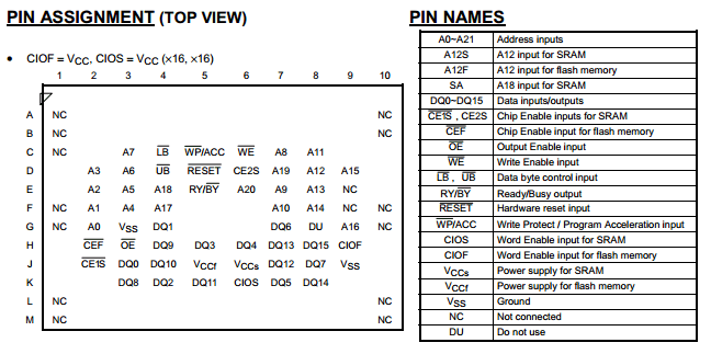
 

TH50VSF2580AASB datasheet

TH50VSF2580AASB Datasheet


Related articles across the web

LH7A404 Datasheet – 32-Bit System-on-Chip ( PDF )

Part Number: LH7A404

Function: 32-Bit System-on-Chip

Package: 324-Pin LFBGA Type

Manufacturer: NXP Semiconductors., Sharp

Pinouts:

LH7A404 datasheet


Description

The advent of 3G technology opens up a wide range of multimedia applications inmobile information appliances.

The LH7A404 is designed from the ground up with a 32-bit ARM922 Core to provide high processing performance, low power consumption, and a high level of integration. Features include 80 kB on-chip SRAM, fully static design, power management unit, low voltage (1.8 V Core, 3.3 V I/O) and on-chip PLL.


Features

1. 32-bit ARM9TDMI RISC Core

(1) 16 kB Cache: 8 kB Instruction and 8 kB Data Cache

(2) MMU (Windows CE™ Enabled)

(3) Up to 266 MHz; See Table 1 for speed options

2. 80 kB On-Chip Static RAM

3. Vectored Interrupt Controller

4. External Bus Interface

(1) Up to 133 MHz; See Table 1 for bus speed options

(2) Asynchronous and Synchronous interface RAM, Flash, PC Card and CompactFlash

5. Clock and Power Management

(1) 32.768 kHz and 14.7456 MHz Oscillators

(2) Programmable PLL


Other data sheets are available within the file:

LH7A404-N0F-000, LH7A404-N0F-092


LH7A404 Datasheet PDF Download

LH7A404 pdf

Related articles across the web