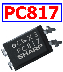
Part Number: LD1117, LD1117V18, LD1117V33, LD1117V50
Function: Adjustable and fixed low drop positive voltage regulator
Package: TO-220, DPAK, SOT-223, SO-8 Type
Manufacturer: STMicroelectronics
Images

Description
The LD1117 is a low drop voltage regulator able to provide up to 800 mA of output current, available even in adjustable version (VREF = 1.25 V). Concerning fixed versions, are offered the following output voltages: 1.2 V, 1.8 V, 2.5 V, 2.85 V, 3.3 V and 5.0 V. The device is supplied in: SOT-223, DPAK, SO-8 and TO-220. The SOT-223 and DPAK surface mount packages optimize the thermal characteristics even offering a relevant space saving effect. High efficiency is assured by NPN pass transistor. In fact in this case, unlike than PNP one, the quiescent current flows mostly into the load. Only a very common 10 μF minimum capacitor is needed for stability.
[…]
Pinout

Features
1. Low dropout voltage (1 V typ.)
2. 2.85 V device performances are suitable for SCSI-2 active termination
3. Output current up to 800 mA
4. Fixed output voltage of: 1.2 V, 1.8 V, 2.5 V, 3.3 V, 5.0 V
5. Adjustable version availability (VREF = 1.25 V)
6. Internal current and thermal limit
7. Available in ± 1 % (at 25 °C) and 2 % in full temperature range
8. Supply voltage rejection: 75 dB (typ.)
Ordering Information
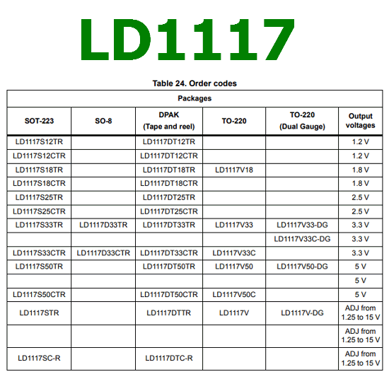
Official Homepage: https://www.st.com/en/power-management/ld1117.html
LD1117 Datasheet