What is BD139? 80V, 1.5A, NPN Transistor ( PDF )

This post explains for the semiconductor BD139.

What is BD139?

This transistor is housed in a TO-126 package and has a maximum collector current of 1.5A, a maximum collector-emitter voltage of 80V, and a maximum power dissipation of 12.5W.

Low noise and high gain characteristics, which make it ideal for use in audio amplifiers and other low-level signal amplification applications. Additionally, its low saturation voltage and fast switching speed make it suitable for use in high-speed switching circuits.

Part Number: BD139, BD137, BD135

Function: 80V, 1.5A, NPN Epitaxial Silicon Transistor

Package: TO-126 3L Type

Manufacturer: Fairchild Semiconductor

Image

BD139 image

Features

1. NPN bipolar junction transistor
2. Low power, medium voltage device
3. Maximum collector current of 1.5A
4. Maximum collector-emitter voltage of 80V
5. Maximum power dissipation of 12.5W
6. Housed in a TO-126 package
7. Low noise and high gain characteristics
8. Low saturation voltage and fast switching speed
9. Suitable for a wide range of applications
10. Complement to BD136, BD138 and BD140 respectively

Advantages Vs Disadvantages

Advantages of BD139:

1. Versatile and widely used in the electronics industry
2. Reliable and cost-effective
3. Ideal for low-level signal amplification applications
4. Suitable for use in high-speed switching circuits
5. Readily available

Disadvantages:

1. Maximum power dissipation of 12.5W may not be sufficient for some high-power applications

2. Maximum collector-emitter voltage of 80V may not be suitable for some high-voltage applications
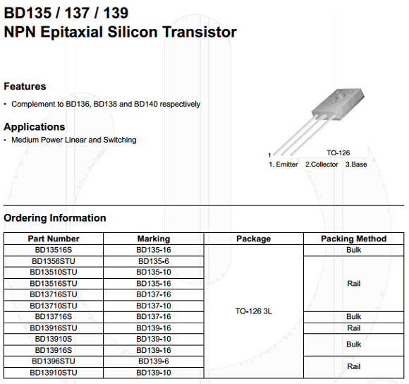
 

BD139 datasheet

Part Number  ->   Marking
BD13516S  ->  BD135-16
BD1356STU  ->  BD135-6
BD13510STU  ->  BD135-10
BD13516STU  ->  BD135-16
BD13716STU  ->  BD137-16
BD13710STU  ->  BD137-10
BD13716S  ->  BD137-16
BD13916STU  ->  BD139-16
BD13910S  ->  BD139-10
BD13916S  ->  BD139-16
BD1396STU  ->  BD139-6
BD13910STU  ->  BD139-10

Absolute maximum ratings ( Ta=25°C )

1. Collector to Base Voltage: Vcbo = 80 V

2. Collector to Emitter Voltage: Vceo = 80 V

3. Emitter to Base Voltage: Vebo = 5 V

4. Collector Current: Ic = 1.5 A

5. Collector Dissipation : Pc = 12.5 W

6. Junction Temperature: Tj = 150°C

7. Storage Temperature: Tsg = -65 ~ +150°C


Applications:

1. Medium Power Linear and Switching


BD139 Datasheet

BD139 fairchild pdf


Related articles across the web

IRF740 Datasheet – N-Channel, 400V, 10A, Power MOSFET

What is IRF740?

This is one of the types of MOSFETs and is a kind of transistor. This is a power MOSFET used for switching and amplification applications. It is an N-channel MOSFET with a voltage rating of 400V and a current rating of 10A.

Function: N-CHANNEL 400V, 0.48 Ohm, 10 A, PowerMESH MOSFET

Package: TO-220 Type

Manufacturer: STMicroelectronics

See the preview image and the IRF740 Datasheet file for more information.

Image

IRF740 datasheet transistor

Description

The IRF740 is N-Channel, 400V, 10A, Power MOSFET.

The PowerMESH II is the evolution of the first generation of MESH OVERLAY. The layout refinements introduced greatly improve the Ron*area figure of merit while keeping the device at the leading edge for what concerns swithing speed, gate charge and ruggedness.

Pinouts:

IRF740 datasheet

Features

1. Exceptional dv/dt capability
2. 100% avalanche tested
3. Low gate charge
4. Very low intrinsic capacitances

Advantages

1. Its TO-220 package provides good thermal dissipation and makes it easy to mount on a heatsink.
2. It has a high voltage rating compared to the IRF640, making it suitable for high-voltage applications.

Disadvantages

1. The IRF740 has a relatively high gate capacitance, which may limit its use in high-frequency switching applications.

2. It is an N-channel MOSFET, which means it requires a positive gate voltage to turn on, making it incompatible with some circuits that require a negative gate voltage.


Applications

1. HIGH CURRENT SWITCHING
2. UNINTERRUPTIBLE POWER SUPPLY (UPS)
3. DC/DC COVERTERS FOR TELECOM, INDUSTRIAL, AND LIGHTING EQUIPMENT.

components


Absolute Maximum Ratings (Ta = 25°C)

1. Drain to source voltage: VDSS = 400 V
2. Gate to source voltage: VGSS = ± 20 V
3. Drain current: ID = 1.0 A
4. Drain power dissipation : PD = 125 W
8. Channel temperature: Tch = 150 °C
9. Storage temperature: Tstg = -65 to +150 °C


Other data sheets are available within the file: IRF740FI

IRF740 Datasheet PDF Download

IRF740 pdf

Related articles across the web