Part Number: MPC9449
Function: 3.3 V/2.5 V 1:15 PECL/LVCMOS Clock Fanout Buffer
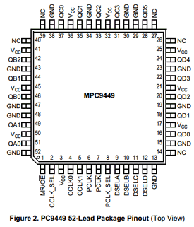
Package: 52-Lead Type
Manufacturer: Motorola, Renesas
Image:

Description
The MPC9449 is a 3.3 V or 2.5 V compatible, 1:15 clock fanout buffer targeted for high performance clock tree applications. With output frequencies up to 200 MHz and output skews less than 200 ps the device meets the needs of the most demanding clock applications.
Block Diagram
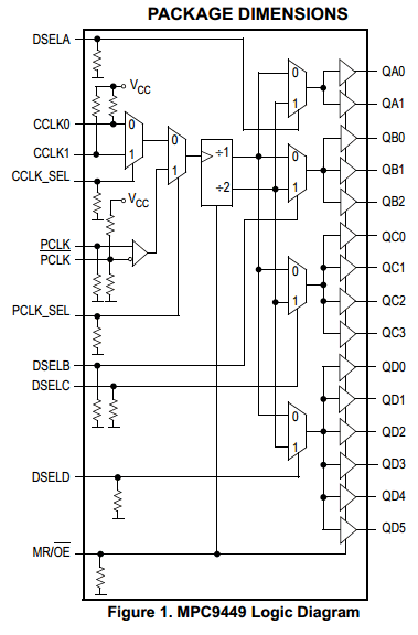
The MPC9449 is specifically designed to distribute LVCMOS compatible clock signals up to a frequency of 200 MHz. The device has 15 identical outputs, organized in four output banks. Each output bank provides a retimed or frequency divided copy of the input signal with a near zero skew. The output buffer supports driving of 50Ω terminated transmission lines on the incident edge: each output is capable of driving either one parallel terminated or two series terminated transmission lines.
Pinout
Features
• 15 LVCMOS compatible clock outputs
• Two selectable LVCMOS and one differential LVPECL compatible clock inputs
• Selectable output frequency divider (divide-by-one and divide-by-two)
• Maximum clock frequency of 200 MHz
• Maximum clock skew of 200 ps
• High-impedance output control
Other data sheets are available within the file: MPC-9449
MPC9449 Datasheet PDF Download