NJW21194G Datasheet – 16A, 250V, NPN Transistor

NJW21194G is a high-speed, high-current, NPN bipolar junction transistor (BJT) designed for use in audio amplifier applications.

Function: 16A, 250V, 200W, NPN Power Transistor

Package: TO-3P Type

Manufacturer: ON Semiconductors

Image

NJW21194G datasheet

Description

The NJW21193G and NJW21194G utilize Perforated Emitter technology and are specifically designed for high power audio output, disk head positioners and linear applications.

Features

• Total Harmonic Distortion Characterized

• High DC Current Gain

• Excellent Gain Linearity

• High SOA

• These Devices are Pb−Free and are RoHS Compliant

Pinouts

NJW21194G pinout

Absolute maximum ratings ( Ta=25°C )

1. Collector to Base Voltage: Vcbo = 250 V

2. Collector to Emitter Voltage: Vceo = 400 V

3. Emitter to Base Voltage: Vebo = 5 V

4. Collector Current: Ic = 16 A

5. Total Dissipation: Pd = 200 W

6. Junction Temperature: Tj = -65 ~ +150°C150°C

7. Storage Temperatue: Tsg = -65 ~ +150°C


Applications

1. Audio amplifier circuits, including high-fidelity audio amplifiers

2. Professional audio equipment, power amplifiers for speakers

Other data sheets within the file : PNP Type ( NJW21193G )

NJW21194G Datasheet PDF

BGU8052 Datasheet – Low Noise High Linearity Amplifier

BGU8052 is a low-noise amplifier (LNA) IC designed for use in radio frequency (RF) applications.

Function: Low Noise High Linearity Amplifier

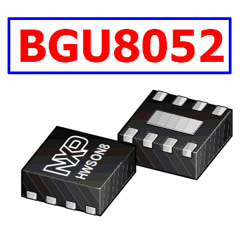
Package: HWSON8, 2mm × 2 mm × 0.75 mm 8-terminal plastic thin small outline package Type

Manufacturer: NXP Semiconductors

Image

BGU8052 datasheet pdf

Description

The BGU8052 is, also known as the BGTS1001M, a low noise high linearity amplifier for wireless infrastructure applications, equipped with fast shutdown to support TDD systems. The LNA has a high input and output return loss and is designed to operate between 1.5 GHz and 2.5 GHz.

Features

• Low noise performance: NF = 0.50 dB

• High linearity performance: IP3O = 36 dBm

• High input return loss > 15 dB

• High output return loss > 20 dB

• Unconditionally stable up to 20 GHz

• Programmable bias current (via resistor)

• ESD protection on all terminals

• Moisture sensitivity level 1

• Fast shut down to support TDD systems

• 3 V to 5 V single supply

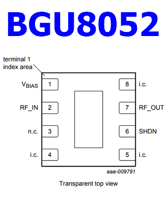
Pinouts

BGU8052 pinout

1. VBIAS,  bias voltage

2. RF_IN,  RF input

3. n.c.,  not connected

4, 5, 8. i.c.,  internally connected. Can be grounded or left open in the application.

6. SHDN,  shutdown

7. RF_OUT,  RF output

Exposed die pad. GND,  ground

Applications

• Wireless infrastructure

• Low noise and high linearity applications

• LTE, W-CDMA, CDMA, GSM

• General-purpose wireless applications

• TDD or FDD systems

• Suitable for small cells

BGU8052 Datasheet PDF

BGU8052 pdf