BU3150 PDF – 800V, 3A, NPN Transistor

Part Number: BU3150

Function: 800V, 3A, NPN Transistor

Package: TO-220A type

Manufacturer: Shenzhen Shangyue Electronics , Jingdao Electronic

Images:

BU3150 pinout


Description

BU3150 is 800V, 3A, NPN transistor. This is a high-voltage bipolar junction transistor designed for power switching applications, supplied in a TO-220A package suitable for efficient heat dissipation. It offers high voltage capability, fast switching speed, and stable operation at elevated temperatures, making it appropriate for demanding power environments.

Features

1. High voltage capability

2. Features of good high temperature

3. High switching speed

Absolute maximum ratings ( Ta=25°C )

1. Collector to Base Voltage: Vcbo = 1100 V

2. Collector to Emitter Voltage: Vceo = 800 V

3. Emitter to Base Voltage: Vebo = 9 V

4. Collector Current: Ic = 3 A

5. Collector Dissipation : Pc = 2 W

6. Junction Temperature: Tj = 150°C

7. Storage Temperature: Tsg = -55 ~ +150°C

BU3150 pdf datasheet

Applications:

1. Computer aided power and Switch-mode power supplies

BU3150 PDF Datasheet

C2655 Transistor – 50V, 2A, NPN, Power Amplifier ( PDF )

This post explains for the transistor.

Part Number: C2655, 2SC2655

Function: 50V, 2A, Silicon NPN Transistor

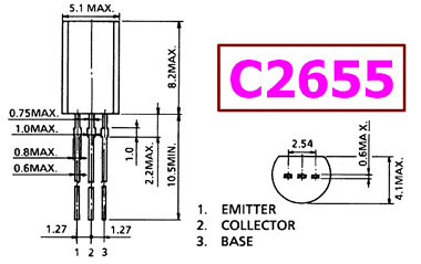
Package: TO-92MOD Type

Manufacturer: Toshiba

See the preview image and the PDF file for more information.

C2655 transistor Image

C2655 transistor

Description

The C2655 is a medium-power NPN silicon transistor designed for both linear amplification and switching applications. It offers low saturation voltage, relatively fast switching characteristics, and moderate current capability, making it suitable for audio stages and general-purpose power control circuits.

Features

1. Low saturation voltage: VCE (sat) = 0.5 V (max) (IC = 1 A)

2. High collector power dissipation: PC = 900 mW

3. High-speed switching: tstg = 1.0 μs (typ.)

4. Complementary to 2SA1020.

C2655 Pinout

C2655 datasheet


Absolute maximum ratings ( Ta=25°C )

1. Collector to Base Voltage: Vcbo = 50 V

2. Collector to Emitter Voltage: Vceo = 50 V

3. Emitter to Base Voltage: Vebo = 5 V

4. Collector Current: Ic = 2A

5. Total Dissipation : Pc = 900 mW

6. Junction Temperature: Tj = 150°C

7. Storage Temperature: Tsg = -55 ~ +150°C

Design Notes (Critical Points)

  • Ensure adequate base drive for full saturation
  • Thermal dissipation is a major limitation (900mW max)
  • Use heat sinking or PCB copper area if operating near limits
  • Include flyback diode when driving inductive loads
  • Avoid operation near maximum ratings for reliability

Advantages vs MOSFET

  • Simpler drive requirements (no gate charge considerations)
  • Better linear behavior for analog amplification

Typical Applications

  • Audio power amplifier stages (driver/output stage)
  • Push-pull amplifier circuits
  • Relay drivers and inductive load switching
  • General-purpose power switching
  • Motor control (low power)

Alternative / Equivalent Products

  • 2SC2655 (standard naming variant)
  • BD139 (higher power capability)
  • 2N2222 (lower current applications)
  • 2SC1815 (signal-level use)

Other data sheets are available within the file: 2SC2655

C2655 Datasheet PDF Download

C2655 pdf

Related articles across the web